
Course of Material & Life Science, Division of Advanced Science and Biotechnology
Graduate School of Engineering, Osaka University


Research
Development of new materials and new processes for the broadband and mobile age
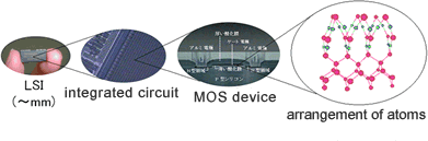
As Internet access has become more and more common, information from anywhere in the world can be obtained from the comfort of our own home. Nowadays, society is moving towards the age of broadband connection. “Broadband”in the internet means “wide road”. Hence, broadband will make roads, which connect your home and cellular phones to the world, several-thousand times wider. In the near future, you may be able to telecommute, or even receive medical care at home without visiting a hospital. In order to realize such a society, electronic devices that are much faster and consume much less power must be developed. Our laboratory aims to develop and evaluate new electronic materials and processes as part of this movement. For instance, an advanced LSI contains several hundred millions of semiconductor devices within a square, which has a side of several millimeters, and the size of each individual device within an LSI is measured in nanometers. Hence, we not only need to precisely control their fabrication processes, but also design the characteristics of the electrodes and substrate materials in order to improve the performance of these devices. Therefore, we are conducting research from a wide range of viewpoints, but our emphasis is on deepening the understanding of the atomic world in order to support the next-generation electronics industry.
Research and development on semiconductor devices to realize high-speed, low-power consumption LSIs
As semiconductor devices scaled down to nanometer regime, the quantum effects become an increasingly important limitation on device performance. In particular, a silicon dioxide film, which is used as a gate insulator of MOS devices, has been thinned down to 1 nm, and the leakage current due to the quantum tunneling effect is currently a major hurdle. To overcome this issue, our laboratory is working on the research and development of materials, structures, and process technologies of a high dielectric constant gate insulator and metal gate electrode, which can provide high drive current without increasing the leakage current. In addition, our research encompasses the realization of devices fabricated on a germanium substrate instead of a silicon substrate, which is currently used as the LSI substrate, due to the superior carrier mobility of germanium. Our studies include: (1) Ge surface cleaning techniques, (2) dielectric film fabrication technology on Ge as well as (3) fabrication and characterization techniques of SGOI (SiGe On Insulator) and GOI (Germanium On Insulator) wafers, which are next-generation semiconductor substrates.
Ideal surface and dielectric film formation technology on wide bandgap semiconductors
Wide bandgap semiconductors such as silicon carbide (SiC) are attracting much attention as semiconductor device materials for power devices to drive the motors of Shinkansen (bullet trains) and hybrid cars, and to transport electrical energy with high efficiency. Silicon (Si) is currently a mainstream material, but employing a wide bandgap material is expected to reduce power consumption as well as carbon dioxide emission. In order to make the best use of the superior properties of wide bandgap materials, new technologies are needed to prepare an ideal surface and to improve the interface characteristics between dielectric films. Our laboratory is developing new processes using high density plasma and exploring new materials in order to realize SiC power devices.
Synchrotron Radiation and its Application to Green Nanoelectronics
Synchrotron radiation (SR) is extremely brilliant, highly directional, and wavelength-tunable - it has been called "dream light." SR has enabled us to see the world on an atomic level. It is variously used for nanotechnology, electronic materials, life science, new medicine development, catalysts, medical application, archaeology, criminal investigation, and more. SR's use in particle physics helps us come close to revealing the origins of the universe. We carry out measurements with the utmost precision on green electronics materials to study atomic order, linkage, and movement using the synchrotron radiation facilities of SPring-8 (with a huge electron accumulation ring with a 1,400m circumference), located in Harima Science Garden City, and the Photon Factory at High Energy Accelerator Research Organization (KEK) in Tsukuba. Synchrotron X-ray Topography visualizes real-space distribution of crystal distortion, crystal defects, crystal face fluctuation by X‐ray diffraction and scattering. It enables measurement of high precision over a large-area which cannot be done in a normal laboratory allowing us to obtain knowledge to enhance performances of next generation semiconductor wafer and solar cell thin film. Furthermore, in synchrotron radiation X-ray photoemission spectroscopy, we precisely evaluate interfacial structure and energy bands structure of ultra-thin film and metal film. We investigate material properties and compatibility and stability of cross-materials, and design nanoelectronics materials.
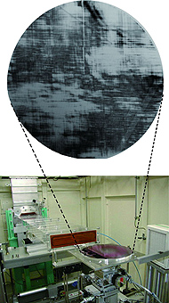 Fig.1 300mm-diameter SOI wafer by synchrotron radiation X-ray topography |
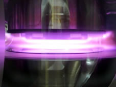
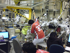 Fig.2 Taken at SPring-8 during an experiment |
Development of high-precision X-ray imaging device that supports the realization of a safe and secure society
Transmission-type X-ray imaging device, which allows observing the inside of the materials non-destructively, is utilized in various fields. In recent years concern over product safety among consumers has been rapidly growing and the responsibility of the manufacturers and the sellers has also been increased. As the results total X-ray inspection is becoming popular especially for foods, beverages, and products for infants. In the field of medical X-ray diagnosis, phase contrast imaging has been actively studied to achieve diagnostic accuracy higher than conventional absorption imaging. This technique is expected in particular for early detection of breast cancer, which one person of 16 Japanese women suffers from. In Watanabe laboratory, we are developing a new type of X-ray imaging device with X-ray source made by semiconductor microfabrication technology and aim to achieve a safe and secure society.
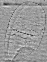
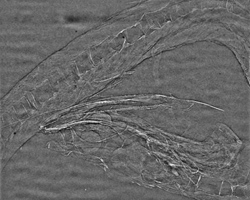
X-ray differential phase contrast images
a piece of rice (left) and a dried young sardine (right)